
Syenta, a next-generation semiconductor company building advanced packaging technology for AI systems, has raised A$37 million (US$26 million) in Series A funding led by Playground Global and Australia’s National Reconstruction Fund (NRF), with participation from Investible, Salus Ventures, Jelix Ventures and Wollemi Capital.
 Follow us
 Follow us
The raise brings total funding to date to A$51.1 million (US$36.4 million), reflecting continued support from leading Australian and global investors as Syenta moves toward commercialisation.
Read More - Kikoff Appoints Chief Financial Officer and Chief Legal Officer
As part of the round, Pat Gelsinger, General Partner at Playground Global and former Chief Executive Officer of Intel, will join Syenta’s Board of Directors, adding deep semiconductor leadership at a time when AI system scaling is increasingly constrained by interconnect and packaging limitations rather than compute alone.
RECOMMENDED FOR YOU

Playground Global’s investment also supports Syenta’s international expansion, including the establishment of US operations in Arizona. NRF’s investment is directed toward strengthening advanced semiconductor manufacturing capability in Australia.
AI scaling is hitting a new constraint layer
As AI systems scale, the limiting factor is increasingly determined by how efficiently chips connect and communicate, rather than compute.
Interconnect bandwidth, packaging density and system-level communication between chips have become central constraints in performance scaling. These challenges sit within advanced packaging, where manufacturing complexity and physical limits are becoming defining bottlenecks for next-generation AI hardware.
At the same time, advanced packaging capacity - the manufacturing step where chips are connected to memory and to each other- remains concentrated in a small number of specialised facilities globally, creating structural supply chain constraints across the semiconductor industry.
A manufacturing approach built for scale
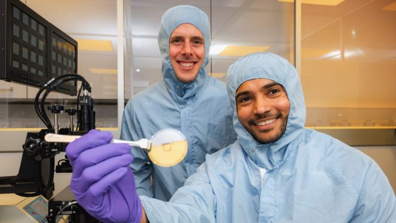
Syenta’s Localized Electrochemical Manufacturing (LEM) technology enables high-density chip-to-chip interconnects within existing semiconductor manufacturing infrastructure.
Early results show micron-scale interconnects and measurable efficiency improvements, including:
- Up to 40% fewer process steps
- No redesign required for existing fabrication infrastructure
- Higher interconnect density enabling improved bandwidth between chips
By working within established manufacturing environments rather than replacing them, LEM is designed to improve scalability in advanced packaging and reduce pressure on constrained global supply chains. The process has been validated through industry programs, including collaborations with leading semiconductor equipment providers.
Playground Global backs the next scaling inflection point
“This is a new way of building high-performance systems at unprecedented scale and power, particularly as AI workloads continue to grow,” said Pat Gelsinger, General Partner at Playground Global.
Read More - LumApps to Buy Comeen to Grow Workplace Experience
Recommended Stories for You

Devin Jacobs Feb 3, 2026
Startuprise Feb 19, 2026

Devin Jacobs Jun 29, 2026

Devin Jacobs May 18, 2026
Startuprise Aug 24, 2025

Trending Stories
Semarion Raises $3.8M in Funding

Hera Raises $27M in Series A Funding Led by Bain Capital Ventures (BCV)

Nebulock Raises $25M in Series A Funding Led by FirstMark
Dr. Sunho Kang joins TeraWatt Technology as Head of Product

Apnimed Secures Up to $150M in Debt Financing

Miravoice Raises $6.3M in Seed Funding

JP Donovan Receives Strategic Investment From Godspeed Capital

Valence AI Raises $5M in Total Funding Led by Differential Ventures

